DDR3/4 & LPDDR4 Design & Layout: Master Your Memory PCB Design! Ddr phy and controller
If you are searching about PCB Design Rules and Tips you've visit to the right web. We have 25 Images about PCB Design Rules and Tips like HW and Layout Design Consideration For DDR3 SDRAM Memory Interfaces, High Speed Pcb Layout Guidelines - Design Talk and also LPDDR4 Design für PCB Entwickler - Zuken GmbH. Here you go:
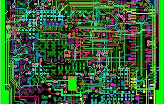
PCB Design Rules And Tips
 www.6pcb.com
PCB Design Rules and Tips
China Mobile DDR4 Lpddr4 Pcb Design And Layout Guidelines Socket
 www.chinax.com
China Mobile DDR4 Lpddr4 Pcb Design And Layout Guidelines Socket ...
LPDDR4 Design Characterisation Runs As An Oscilloscope Complian...
 www.eenewseurope.com
LPDDR4 design characterisation runs as an oscilloscope complian...
LPDDR4 Design Für PCB Entwickler - Zuken GmbH
 www.zuken.com
LPDDR4 Design für PCB Entwickler - Zuken GmbH
Pcb Design Guidelines Mechanical Layer Eurocircuits Eurocircuits Images
 www.tpsearchtool.com
Pcb Design Guidelines Mechanical Layer Eurocircuits Eurocircuits Images
AM6412: EVM的LPDDR4 Layout Design確認 - 处理器论坛 - 处理器 - E2E™ 设计支持
 e2echina.ti.com
AM6412: EVM的LPDDR4 layout design確認 - 处理器论坛 - 处理器 - E2E™ 设计支持
LPDDR4/4x PHY IP For 22nm
 www.design-reuse.com
LPDDR4/4x PHY IP for 22nm
Nine Dot Connects » Altium Designer PCB Editor, Nine Dot Connects, 9dot
 www.ninedotconnects.com
Nine Dot Connects » Altium Designer PCB Editor, Nine Dot Connects, 9dot ...
Circuit Board Design
 ar.inspiredpencil.com
Circuit Board Design
High Speed Pcb Layout Guidelines - Design Talk
 design.udlvirtual.edu.pe
High Speed Pcb Layout Guidelines - Design Talk
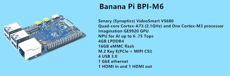
Banana Pi BPI-M6 With Senary(Synaptics) VS680 Design ,onboard 4G LPDDR4
 forum.banana-pi.org
Banana Pi BPI-M6 with Senary(Synaptics) VS680 design ,onboard 4G LPDDR4 ...
Simulation VIP For LPDDR4 | Cadence
 www.cadence.com
Simulation VIP for LPDDR4 | Cadence
LPDDR4 Design Für PCB Entwickler - Zuken GmbH
 www.zuken.com
LPDDR4 Design für PCB Entwickler - Zuken GmbH
Using SDRAM Vs. DDR RAM In Your PCB Design | Blog | Altium Designer
 resources.altium.com
Using SDRAM vs. DDR RAM in Your PCB Design | Blog | Altium Designer
What Is Fan Out In Pcb At Kenneth Neilson Blog
 storage.googleapis.com
What Is Fan Out In Pcb at Kenneth Neilson blog
(PDF) Jacinto 7 LPDDR4 Board Design And Layout Guidelines (Rev. B
 pdfslide.net
(PDF) Jacinto 7 LPDDR4 Board Design and Layout Guidelines (Rev. B ...
DDR PHY And Controller | Cadence
 www.cadence.com
DDR PHY and Controller | Cadence
PCB Routing Guidelines For DDR4 Memory Devices And Impedance | Blog
 resources.altium.com
PCB Routing Guidelines for DDR4 Memory Devices and Impedance | Blog ...
DDR3 PCB Design And Routing: A Comprehensive Guide
 www.linkedin.com
DDR3 PCB Design and Routing: A Comprehensive Guide
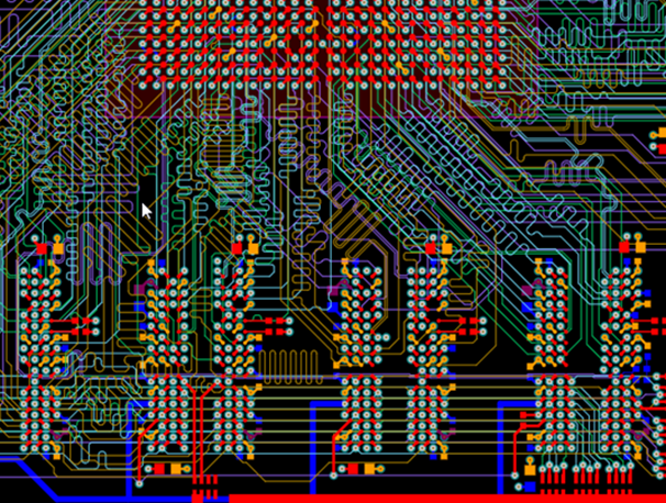
LPDDR4 Design And Layout Tutorial Series #2/5 | FANOUT | Altium
 www.youtube.com
LPDDR4 Design and Layout tutorial series #2/5 | FANOUT | Altium ...
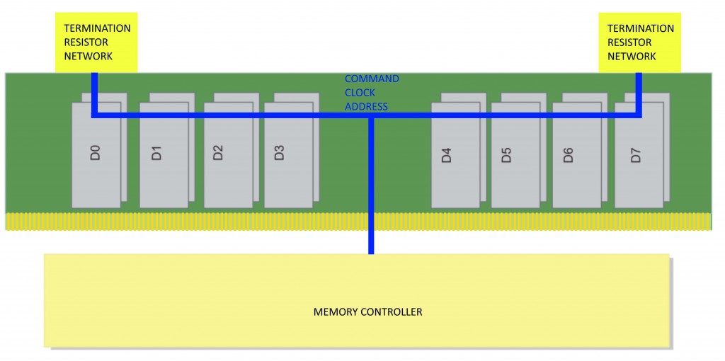
HW And Layout Design Consideration For DDR3 SDRAM Memory Interfaces
 www.scribd.com
HW and Layout Design Consideration For DDR3 SDRAM Memory Interfaces ...
LPDDR4 Design And Layout Tutorial - ADVANCED PCB Design Rules - YouTube
 www.youtube.com
LPDDR4 Design and Layout Tutorial - ADVANCED PCB Design Rules - YouTube
DDR3 Pcb Design Routing - Electrical Engineering Stack Exchange
 electronics.stackexchange.com
DDR3 pcb design routing - Electrical Engineering Stack Exchange
Nine Dot Connects » DDR3, DDR4, LPDDR4 Design And Layout Services, Nine
 www.ninedotconnectssandbox.com
Nine Dot Connects » DDR3, DDR4, LPDDR4 Design and Layout Services, Nine ...
DDR3 Layout Vs Memory Chip Fitting : R/robertferanec
 www.reddit.com
DDR3 layout vs Memory chip fitting : r/robertferanec
Pcb routing guidelines for ddr4 memory devices and impedance. Banana pi bpi-m6 with senary(synaptics) vs680 design ,onboard 4g lpddr4. Ddr3 layout vs memory chip fitting : r/robertferanec