Ground Fill Taking Too Much Space? Optimize Your PCB Layout! Out of pcb space,
If you are searching about PCB Layout Design Tips – Grounding Considerations – PCB HERO you've visit to the right place. We have 25 Images about PCB Layout Design Tips – Grounding Considerations – PCB HERO like PCB Layout Optimisation | PDF | Electrostatic Discharge | Printed, Background in PCB-layout Style with Empty Space for Your Text. Stock and also How to choose the best way to fill the hole for your PCB design?. Here you go:
PCB Layout Design Tips – Grounding Considerations – PCB HERO
 www.pcb-hero.com
PCB Layout Design Tips – Grounding Considerations – PCB HERO
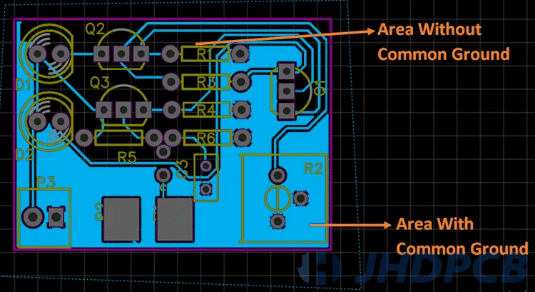
The Role And Design Guidelines Of PCB Ground Plane. - Jhdpcb
 jhdpcb.com
The Role And Design Guidelines Of PCB Ground Plane. - Jhdpcb
How You Can Optimize A PCB Panel Format - Servamega
 servamega.com
How you can Optimize a PCB Panel Format - Servamega
How To Optimize The PCB Enclosure And Board Layout As The Pro?
 www.linkedin.com
How to optimize the PCB Enclosure and Board Layout as the Pro?
Tips For Improving Your PCB Layout Efficiency • Itechsoul | Improve
 www.pinterest.com
Tips for Improving Your PCB Layout Efficiency • Itechsoul | Improve ...
Out Of PCB Space, - Page 1
 www.eevblog.com
Out of PCB space, - Page 1
How To Optimize And Reduce PCB Size
 www.linkedin.com
How to optimize and reduce PCB size
Out Of PCB Space, - Page 3
 www.eevblog.com
Out of PCB space, - Page 3
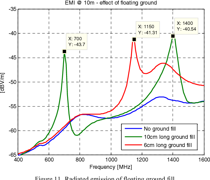
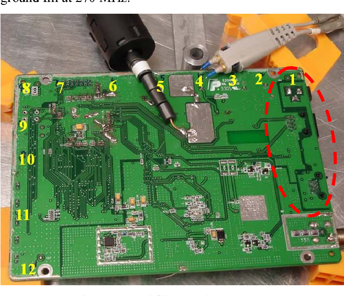
Figure 2 From PCB Ground Fill Design Guidelines For Radiated EMI
 www.semanticscholar.org
Figure 2 from PCB ground fill design guidelines for radiated EMI ...
Ground Plane Pcb Stock Photos And Pictures - 33 Images | Shutterstock
 www.shutterstock.com
Ground Plane Pcb Stock Photos and Pictures - 33 Images | Shutterstock
PCB Layout Design Tips – Grounding Considerations – PCB HERO
 www.pcb-hero.com
PCB Layout Design Tips – Grounding Considerations – PCB HERO
Pcb Design - How Do I Decide On A Proper PCB Ground Layout
 electronics.stackexchange.com
pcb design - How do I decide on a proper PCB ground layout ...
How To Choose The Best Way To Fill The Hole For Your PCB Design?
 www.linkedin.com
How to choose the best way to fill the hole for your PCB design?
PCB Layout Optimisation | PDF | Electrostatic Discharge | Printed
 www.scribd.com
PCB Layout Optimisation | PDF | Electrostatic Discharge | Printed ...
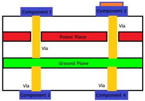
How To Improve Your PCB Layout – Power Planes : R/robertferanec
 www.reddit.com
How To Improve Your PCB Layout – Power Planes : r/robertferanec
PCB Layout Design Tips – Grounding Considerations – PCB HERO
 www.pcb-hero.com
PCB Layout Design Tips – Grounding Considerations – PCB HERO
Quick Fix System Restore Taking Up Too Much Space
 wearableworld.co
Quick Fix System Restore Taking Up Too Much Space
PCB Layout Steps To Maximize Performance
 www.linkedin.com
PCB Layout Steps to Maximize Performance
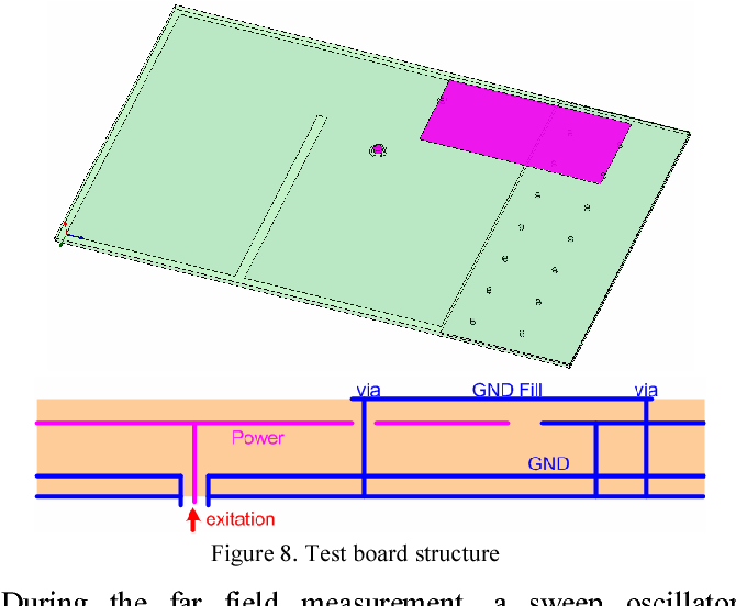
Figure 1 From PCB Ground Fill Design Guidelines For Radiated EMI
 www.semanticscholar.org
Figure 1 from PCB ground fill design guidelines for radiated EMI ...
PCB Layout Tips And Tricks: Use A Ground Plane Whenever Possible – ElexHere
 elexhere.com
PCB Layout Tips and Tricks: Use a Ground Plane Whenever Possible – ElexHere
Basics Of PCB Layout: Components, Traces, And Ground Planes | Viasion
 www.viasion.com
Basics of PCB Layout: Components, Traces, and Ground Planes | Viasion
Background In PCB-layout Style With Empty Space For Your Text. Stock
 www.dreamstime.com
Background in PCB-layout Style with Empty Space for Your Text. Stock ...
Top PCB Layout Mistakes To Avoid And How Your CM Can Help
 www.linkedin.com
Top PCB Layout Mistakes to Avoid and How Your CM Can Help
Figure 2 From PCB Ground Fill Design Guidelines For Radiated EMI
 www.semanticscholar.org
Figure 2 from PCB ground fill design guidelines for radiated EMI ...
Ground Layout | Forum For Electronics
Ground layout | Forum for Electronics
Pcb layout design tips – grounding considerations – pcb hero. Pcb layout design tips – grounding considerations – pcb hero. How you can optimize a pcb panel format